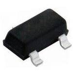
SI2325DS-T1-GE3, MOSFETs -150V Vds 20V Vgs SOT-23

Изображения служат только для ознакомления,
см. техническую документацию
см. техническую документацию

1 250 ֏
от 10 шт. —
980 ֏
от 100 шт. —
710 ֏
от 500 шт. —
560 ֏
Добавить в корзину 1 шт.
на сумму 1 250 ֏
Описание
Unclassified
SI2 Series TrenchFET® Power MOSFETsVishay SI2 Series TrenchFET® Power MOSFETs are N-channel MOSFETs designed with 30V V (ds) and are 100% tested gate resistance(R g ). These MOSFETs have gate resistance tested for 1MHz frequency with 0.2Ω to 1.4Ω. These SI2 series MOSFETs operate from -55 C to 150 C junction and storage temperature. The SI2 series are ideal for DC/DC converter, Load switch, and power management.
Технические параметры
| Brand: | Vishay Semiconductors |
| Channel Mode: | Enhancement |
| Configuration: | Single |
| Factory Pack Quantity: Factory Pack Quantity: | 3000 |
| Fall Time: | 11 ns |
| Id - Continuous Drain Current: | 530 mA |
| Manufacturer: | Vishay |
| Maximum Operating Temperature: | +150 C |
| Minimum Operating Temperature: | -55 C |
| Mounting Style: | SMD/SMT |
| Number of Channels: | 1 Channel |
| Package / Case: | SOT-23-3 |
| Part # Aliases: | SI2325DS-T1-BE3 SI2325DS-GE3 |
| Pd - Power Dissipation: | 750 mW |
| Product Category: | MOSFET |
| Product Type: | MOSFET |
| Qg - Gate Charge: | 7.7 nC |
| Rds On - Drain-Source Resistance: | 1.2 Ohms |
| Rise Time: | 11 ns |
| Series: | SI2 |
| Subcategory: | MOSFETs |
| Technology: | Si |
| Tradename: | TrenchFET |
| Transistor Polarity: | P-Channel |
| Transistor Type: | 1 P-Channel |
| Typical Turn-Off Delay Time: | 16 ns |
| Typical Turn-On Delay Time: | 7 ns |
| Vds - Drain-Source Breakdown Voltage: | 150 V |
| Vgs - Gate-Source Voltage: | -20 V, +20 V |
| Vgs th - Gate-Source Threshold Voltage: | 4.5 V |
| Automotive | No |
| Channel Mode | Enhancement |
| Channel Type | P |
| Configuration | Single |
| ECCN (US) | EAR99 |
| EU RoHS | Compliant |
| Lead Shape | Gull-wing |
| Maximum Continuous Drain Current (A) | 0.53 |
| Maximum Continuous Drain Current on PCB @ TC=25°C (A) | 0.53 |
| Maximum Drain Source Resistance (mOhm) | 1200@10V |
| Maximum Drain Source Voltage (V) | 150 |
| Maximum Gate Source Leakage Current (nA) | 100 |
| Maximum Gate Source Voltage (V) | ±20 |
| Maximum Gate Threshold Voltage (V) | 4.5 |
| Maximum IDSS (uA) | 1 |
| Maximum Junction Ambient Thermal Resistance on PCB (°C/W) | 166 |
| Maximum Operating Temperature (°C) | 150 |
| Maximum Positive Gate Source Voltage (V) | 20 |
| Maximum Power Dissipation (mW) | 1250 |
| Maximum Power Dissipation on PCB @ TC=25°C (W) | 1250 |
| Maximum Pulsed Drain Current @ TC=25°C (A) | 1.6 |
| Minimum Gate Threshold Voltage (V) | 2.5 |
| Minimum Operating Temperature (°C) | -55 |
| Mounting | Surface Mount |
| Number of Elements per Chip | 1 |
| Operating Junction Temperature (°C) | -55 to 150 |
| Packaging | Tape and Reel |
| Part Status | Active |
| PCB changed | 3 |
| Pin Count | 3 |
| PPAP | No |
| Process Technology | TrenchFET |
| Product Category | Power MOSFET |
| Standard Package Name | SOT |
| Supplier Package | SOT-23 |
| Typical Fall Time (ns) | 11 |
| Typical Gate Charge @ 10V (nC) | 7.7 |
| Typical Gate Charge @ Vgs (nC) | 7.7@10V |
| Typical Gate Plateau Voltage (V) | 5 |
| Typical Gate to Drain Charge (nC) | 2.5 |
| Typical Gate to Source Charge (nC) | 1.5 |
| Typical Input Capacitance @ Vds (pF) | 340@25V |
| Typical Output Capacitance (pF) | 30 |
| Typical Reverse Recovery Charge (nC) | 90 |
| Typical Reverse Transfer Capacitance @ Vds (pF) | 16@25V |
| Typical Rise Time (ns) | 11 |
| Typical Turn-Off Delay Time (ns) | 16 |
| Typical Turn-On Delay Time (ns) | 7 |
| Вес, г | 0.01 |
Техническая документация
Datasheet
pdf, 163 КБ


