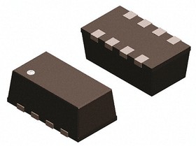
P-Channel MOSFET, 9.9 A, 30 V, 8-Pin PowerPAK ChipFET SI5419DU-T1-GE3
Изображения служат только для ознакомления,
см. техническую документацию
см. техническую документацию
307 ֏
Кратность заказа 20 шт.
Добавить в корзину 20 шт.
на сумму 6 140 ֏

Описание
Semiconductors\Discrete Semiconductors\MOSFETs
Trans MOSFET P-CH 30V 9.9A 8-Pin PowerPAK ChipFET T/R
Технические параметры
| Channel Mode | Enhancement |
| Channel Type | P |
| Maximum Continuous Drain Current | 9.9 A |
| Maximum Drain Source Resistance | 33 mΩ |
| Maximum Drain Source Voltage | 30 V |
| Maximum Gate Source Voltage | -20 V, +20 V |
| Maximum Operating Temperature | +150 °C |
| Maximum Power Dissipation | 31 W |
| Minimum Gate Threshold Voltage | 1.2V |
| Minimum Operating Temperature | -55 °C |
| Mounting Type | Surface Mount |
| Number of Elements per Chip | 1 |
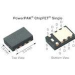
| Package Type | PowerPAK ChipFET |
| Pin Count | 8 |
| Transistor Configuration | Single |
| Transistor Material | Si |
| Typical Gate Charge @ Vgs | 30 nC @ 10 V |
| Width | 1.98mm |
| Automotive | No |
| Configuration | Single |
| ECCN (US) | EAR99 |
| Lead Shape | No Lead |
| Maximum Continuous Drain Current (A) | 9.9 |
| Maximum Drain Source Resistance (mOhm) | 20@10V |
| Maximum Drain Source Voltage (V) | 30 |
| Maximum Gate Source Voltage (V) | ±20 |
| Maximum Operating Temperature (°C) | 150 |
| Maximum Power Dissipation (mW) | 3100 |
| Minimum Operating Temperature (°C) | -55 |
| Mounting | Surface Mount |
| Operating Junction Temperature (°C) | -55 to 150 |
| Packaging | Tape and Reel |
| Part Status | Active |
| PCB changed | 8 |
| PPAP | No |
| Process Technology | TrenchFET |
| Product Category | Power MOSFET |
| Standard Package Name | Chip FET |
| Supplier Package | PowerPAK ChipFET |
| Typical Fall Time (ns) | 16|12 |
| Typical Gate Charge @ 10V (nC) | 30 |
| Typical Gate Charge @ Vgs (nC) | 15.5@4.5V|30@10V |
| Typical Input Capacitance @ Vds (pF) | 1400@15V |
| Typical Rise Time (ns) | 33|10 |
| Typical Turn-Off Delay Time (ns) | 30|40 |
| Typical Turn-On Delay Time (ns) | 47|10 |


